WaveLink
WaveLink
WaveLink
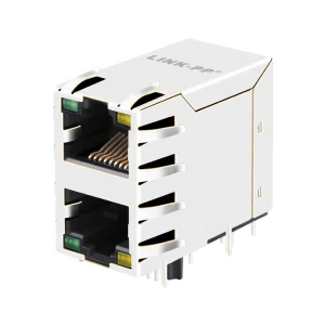
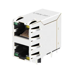
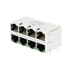
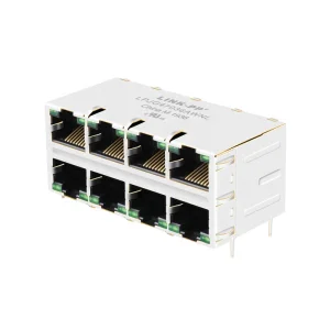
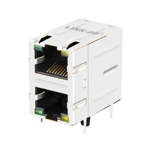
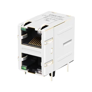
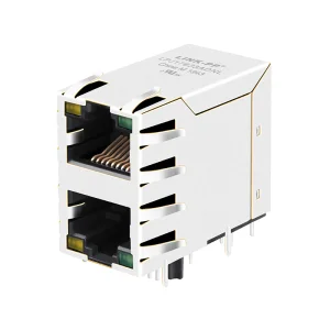
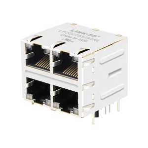
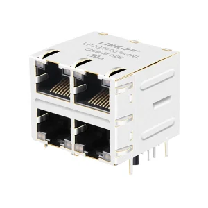
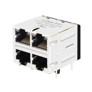
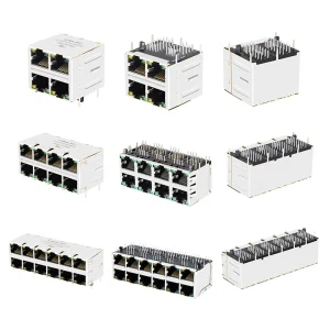
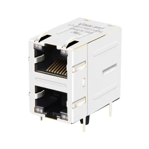
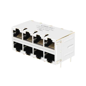
Select configurations with advanced integrated magnetics (MagJack), multi-port density, and internal EMI shielding.
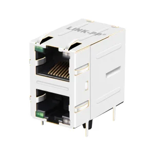
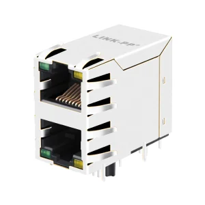
A global standard optical transceiver and high-speed electrical connectivity partner operating from China's high-tech manufacturing corridors.
WaveLink Optoelectronics Co., Ltd. is a professional manufacturer specializing in high-performance optical transceivers and fiber optic connectivity solutions for telecom and data center applications.
Founded in 2016, WaveLink has built a strong reputation in the global optoelectronics industry with a modern production base covering approximately 12,800㎡. The company generates an annual export revenue of around USD 18 million, supported by 7 years of export experience and 12 years of overall industry expertise.
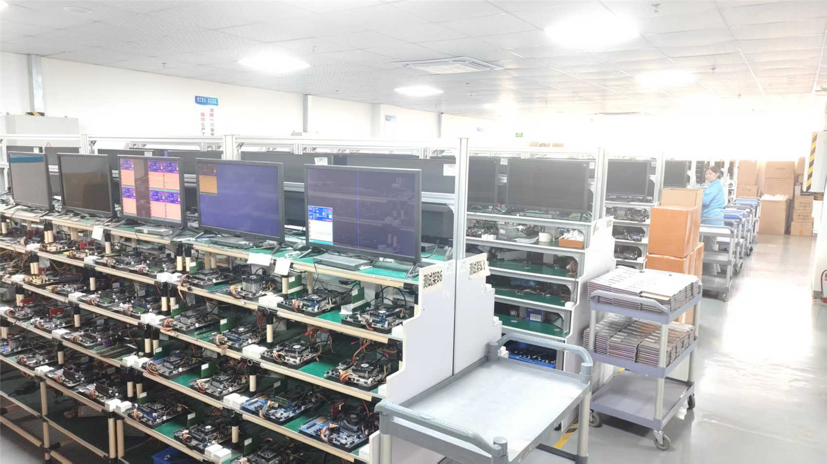
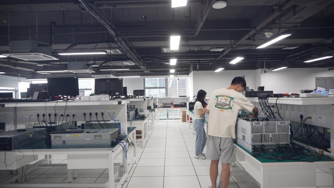
WaveLink operates a strict quality management system, including 100% performance testing, optical signal integrity testing, and high-temperature aging tests. Product inspection methods include automated optical testing, manual visual inspection, and real-time digital calibration systems. The quality control team consists of 45 dedicated QC engineers ensuring product stability and compliance with international standards.
With a solid trade background in global B2B electronics export, WaveLink primarily serves markets in North America, Europe, Southeast Asia, and the Middle East. The company maintains partnerships with more than 1,200 upstream supply chain partners, enabling stable component sourcing and fast production scaling.


Understanding high-density, signal integrity, and manufacturing matrices in high-speed digital systems.
Strategic clustering of copper alloy drawing, precision mold injection, and high-frequency automated winding machines allows Chinese factories to scale RJ45 connectors with unmatched speed-to-market. The robust domestic supply chain reduces reliance on third-party components, cushioning global partners against macro-economic supply shocks.
With WiFi 6E, WiFi 7, and IoT endpoint expansion, classical gigabit copper endpoints are outdated. Modern PCB Stacked Integrated Connectors are redesigned to handle Cat6a frequencies up to 500 MHz, incorporating localized internal cross-talk shields between stacked channels to maintain pristine SNR margins.
Delivering up to 90W per port over stacked interfaces requires strict thermal profiling. Advanced copper alloys coupled with 50u" gold plating ensure contact resistance remains below 20 mΩ, preventing thermal degradation and signal droop inside heavy-duty modular switches.
Procurement teams do not merely buy connectors; they mitigate channel noise and design footprint limitations. A 2x4 configuration saves up to 48% more PCB edge space than eight discrete coplanar RJ45 ports. Incorporating internal transformer windings directly into the connector (Integrated Connector Module - ICM) reduces component counts, mitigates parasitic capacitance, and isolates electrical surges before they cross the main controller threshold.
Modern enterprises prioritize long-term component lifecycle stability over short-term price benefits. Connectors must withstand 750 mechanical mating cycles minimum while preserving contact geometry under variable vibration patterns. WaveLink's engineering approach resolves these issues through intensive high-temperature aging chambers and 100% automated optical inspection systems.
Additionally, complying with environmental standards like RoHS 3 and REACH is no longer optional. Product traceability from raw phosphor bronze and copper plating to packaging materials guarantees frictionless clearance in highly regulated North American and European sectors.
With approximately 180 new product models introduced over the last fiscal cycle, our research team of 220 dedicated engineers adapts standard stacked footprints to accommodate custom LED positions, modified tab orientations (Tab-up vs. Tab-down), special EMI fingers, and vertical heights matching unique chassis requirements.
High-speed stacked models featuring specialized LED combinations, variable PoE power profiles, and localized footprint architectures.
Common technical clarifications regarding stacked port design, EMI shielding, and OEM adaptation capabilities.